The global semiconductor industry stands at a pivotal juncture, continuously evolving to meet the insatiable demands of an increasingly digitized world. As we approach 2026, the landscape of chip production is undergoing a profound transformation, driven by geopolitical shifts, technological breakthroughs, and an intensified focus on sustainability and talent. This period marks The Reshaping of Semiconductor Manufacturing in 2026, characterized by strategic investments and a re-evaluation of traditional supply chain models.
Geopolitical Realignment and Supply Chain Diversification
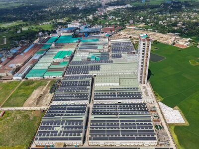
The semiconductor manufacturing sector is experiencing an unprecedented wave of regionalization, largely spurred by the supply chain disruptions witnessed during the COVID-19 pandemic and escalating geopolitical tensions. Governments worldwide are actively incentivizing domestic chip production to enhance national security and economic resilience. For instance, the U.S. CHIPS and Science Act, enacted in 2022, allocates approximately $52.7 billion in subsidies for semiconductor research, development, manufacturing, and workforce development. This has already catalyzed significant investments, such as TSMC's commitment to build multiple advanced fabs in Arizona, with an initial investment exceeding $40 billion, projected to produce 4nm and eventually 3nm chips. Similarly, Intel announced plans for a $20 billion (estimated) manufacturing facility in Ohio, aimed at boosting American chip production capacity.
Parallel efforts are underway in Europe and Asia. The European Chips Act, proposed in 2022, aims to mobilize €43 billion in public and private investment to double the EU's share in global semiconductor production to 20% by 2030. This initiative supports projects from companies like Intel, which is expanding its manufacturing presence in Germany with a planned €17 billion (estimated) investment for two new fabs, and STMicroelectronics, which is building a new 300mm wafer fab in Italy. Japan has also joined this global push, offering substantial subsidies to attract foreign investment, notably securing a commitment from TSMC to build a new fab in Kumamoto with Sony and Denso, focusing on mature and specialty technologies to bolster its domestic supply chain. These multinational investments, spanning billions of dollars, underscore a collective global strategy to diversify manufacturing footprints away from over-reliance on a few key regions, fundamentally altering the geographical distribution of advanced chip production by 2026.
This strategic diversification is not merely about capacity but also about resilience. The goal is to create more robust, localized ecosystems that can withstand future shocks, whether from natural disasters, pandemics, or geopolitical conflicts. Countries are competing fiercely to attract leading-edge foundries and their intricate supply chains, including equipment suppliers (e.g., ASML, Applied Materials, Lam Research) and material providers. This has led to a significant increase in capital expenditures across the industry, with global semiconductor capital spending projected to remain strong, potentially reaching an approximate $150-200 billion annually in the mid-2020s, as new fabs come online and existing ones are upgraded. The long-term implications include more distributed manufacturing, potentially shorter lead times for certain components, and a complex web of interdependent regional hubs rather than a singular global manufacturing center.
Technological Frontiers: Advanced Nodes, Packaging, and AI Integration
Beyond geographical shifts, The Reshaping of Semiconductor Manufacturing in 2026 is profoundly influenced by relentless technological advancement. The industry continues its march towards smaller process nodes, with leading foundries like TSMC and Samsung targeting 2nm and even 1.8nm production by 2025-2026. Achieving these ultra-small geometries necessitates increasingly sophisticated manufacturing techniques, most notably High-NA Extreme Ultraviolet (EUV) lithography. While current EUV tools are capable of 3nm production, High-NA EUV, with its higher numerical aperture, promises to enable 2nm and below, albeit at significantly higher costs and complexity. ASML, the sole producer of EUV equipment, is at the forefront, with the first High-NA EUV systems expected to be deployed in fabs around this timeframe, representing a monumental leap in patterning capability.
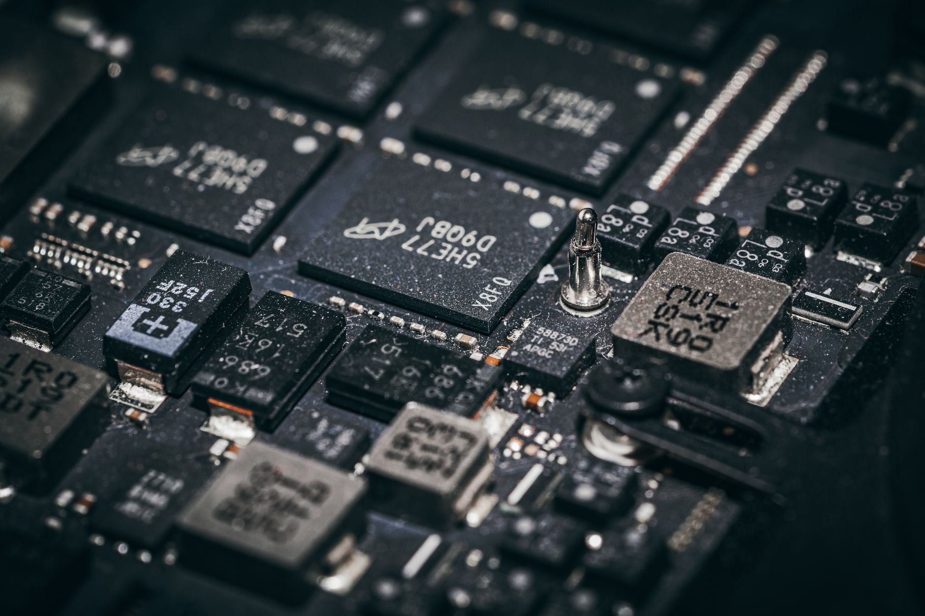
However, the escalating costs and technical hurdles associated with traditional node scaling are driving innovation in advanced packaging technologies. Chiplets, 3D stacking (e.g., High Bandwidth Memory - HBM, logic-on-logic), and heterogeneous integration are becoming critical for performance and power efficiency. Instead of fabricating an entire complex system on a single monolithic die, chiplets allow different functional blocks (CPU, GPU, I/O, memory) to be manufactured separately, often on different process nodes optimized for their specific function, and then integrated into a single package. This modular approach offers greater flexibility, improved yields, and better cost management, especially for high-performance computing (HPC) and AI accelerators. Companies like AMD, Intel, and NVIDIA are heavily investing in these technologies, which are set to become standard practice in high-end processors by 2026, extending Moore's Law equivalent benefits even as transistor scaling slows.
Artificial Intelligence (AI) is also revolutionizing every stage of semiconductor manufacturing, from design and simulation to factory operations and quality control. AI-driven design tools can explore vast design spaces more efficiently, optimizing for performance, power, and area. In the fab, AI algorithms are being deployed for predictive maintenance of complex machinery, real-time process control, and yield enhancement. By analyzing massive datasets from sensors and equipment logs, AI can identify potential issues before they lead to defects, optimize chemical processes, and improve the consistency of production. This intelligent automation not only boosts efficiency but also helps manage the inherent variability and complexity of advanced manufacturing processes. The integration of AI will be a defining characteristic of advanced fabs by 2026, driving unprecedented levels of automation and precision.
- Advanced Lithography: High-NA EUV adoption, despite its immense cost and complexity, will be crucial for pushing the boundaries of transistor density.
- New materials and designs for enhanced performance, including novel transistor architectures and interconnect solutions, will continue to emerge to meet the demands of next-generation computing.
Sustainability, Talent Development, and Operational Excellence
As the semiconductor industry expands, its environmental footprint comes under increasing scrutiny, making sustainability a critical pillar of future manufacturing strategies. Modern fabs are incredibly energy-intensive, consuming vast amounts of electricity, water, and specialized chemicals. By 2026, there will be intensified efforts to reduce this impact. Companies are investing in renewable energy sources for their operations, optimizing water recycling systems to achieve near-zero liquid discharge, and developing more environmentally friendly chemicals and waste treatment processes. Leading manufacturers have set ambitious targets, such as Intel's goal to achieve net-zero greenhouse gas emissions across its global operations by 2040 and TSMC's commitment to use 100% renewable energy for all its fabs by 2050, with significant milestones planned for the mid-2020s. These commitments reflect a growing industry-wide recognition that sustainable practices are not just good for the planet but also crucial for long-term operational viability and public perception.
Another profound challenge facing semiconductor manufacturing is the persistent global talent gap. The demand for highly skilled engineers, technicians, and researchers far outstrips the current supply, a problem exacerbated by the rapid expansion of manufacturing capacity. By 2026, this shortage could become a bottleneck for growth and innovation. Governments, industry associations, and academic institutions are collaborating to address this through various initiatives, including enhanced STEM education programs, specialized university curricula, apprenticeships, and vocational training schemes. For example, the U.S. CHIPS Act includes provisions for workforce development, and many companies are partnering with local universities to establish dedicated research and training centers. Attracting and retaining top talent will be paramount for any region aiming to establish itself as a semiconductor hub, requiring competitive compensation, state-of-the-art facilities, and opportunities for continuous professional development.
Operational excellence, driven by advanced automation and data analytics, will define the competitive edge in 2026. The complexity of modern fabs, with thousands of process steps and millions of data points, demands sophisticated management systems. Beyond AI for process control, the adoption of Industry 4.0 principles – integrating cyber-physical systems, IoT, cloud computing, and big data analytics – is transforming factory floors. Smart manufacturing systems can predict equipment failures, optimize production schedules in real-time, and trace every wafer through its entire journey, ensuring quality and efficiency. This level of interconnectedness and intelligent automation minimizes human error, maximizes throughput, and significantly reduces operational costs, allowing manufacturers to maintain profitability even as R&D and capital expenditures continue to soar. The operational efficiency achieved through these advancements will be a key differentiator in the highly competitive semiconductor landscape.
Key Takeaways
- Regionalization and Resilience: The global semiconductor industry is undergoing a significant shift towards more regionalized supply chains, driven by geopolitical factors and a desire for enhanced resilience. Billions of dollars in government incentives and private investments are fueling the construction of new fabs in North America, Europe, and Asia, aiming to diversify production capacities by 2026.
- Technological Frontier and Advanced Packaging: The relentless pursuit of smaller process nodes (e.g., 2nm, 1.8nm) is pushing the boundaries of lithography with High-NA EUV. Simultaneously, advanced packaging technologies like chiplets and 3D stacking are becoming crucial for extending performance and managing costs, offering a modular approach to high-performance computing.
- Sustainability and Workforce Development: Environmental responsibility is increasingly integrated into manufacturing, with fabs targeting net-zero emissions, optimized water usage, and green practices. Addressing the critical global talent gap through robust education and training programs is also paramount to sustaining the industry's rapid growth and innovation through 2026 and beyond.